PCB Manufacture:
About Us:
KFTRONICS is a reputable electronics manufacturing company that specializes in designing and producing high-quality Printed Circuit Boards (PCBs). With over a decade of experience, we have established a solid reputation for delivering precise, reliable, and cost-effective solutions to clients in industries such as industrial automation, textile electronics, and custom control systems.
Established in 2015, KFTRONICS is dedicated to delivering top-notch PCB solutions that cater to the changing needs of modern electronics at an affordable price without compromising quality. Our PCBs are utilized in various applications, including our popular Jacquard controllers, showcasing our dedication to excellence and longevity.
At KFTRONICS, we utilize advanced manufacturing technology and skilled craftsmanship to provide a wide range of PCB fabrication services. Our offerings include single-sided boards and multi-layer designs, all with tight tolerances, rigorous quality control, and punctual delivery. 10 years of powering connections with precision, quality, and trust.
Our Strengths:
- 10+ years of proven PCB manufacturing expertise
- Fully equipped in-house production with advanced testing and inspection
- Strict quality standards for high reliability and durability
- Customized solutions for specialized applications
- Responsive support and transparent service at every stage
With a strong foundation in experience and a commitment to innovation, KFTRONICS consistently invests in cutting-edge technologies and processes to produce high-quality PCBs that excel in challenging conditions. Whether you're an OEM, system integrator, or electronics innovator, we're your reliable partner for PCBs that bring your ideas to reality.
SERVICES:
Printed Circuit Boards (PCBs) are essential components in electronic devices, providing the foundation for gadgets such as smartphones and satellites. PCB design can be intimidating for beginners, but fear not! KFTRONICS specializes in all aspects of PCB design, creating efficient and reliable layouts that can endure challenging conditions. Trust us to deliver high-quality PCB designs for your projects.
We offer complete solutions for electronic product development, including
- PCB designing
- PCB Reverse engineering
- Rapid prototyping
- PCB fabrication
- PCB Assembly
- Component sourcing
- Embedded firmware development
- Electronics testing
- Enclosure designs.
PCB DESIGN Service:
PCB design is crucial for electronic products, as it is derived from the final product's schematic diagram. It includes circuit layout and component positioning to form an integrated circuit board. A well-crafted schematic diagram, coupled with effective circuit performance and heat dissipation design, can enhance product performance, longevity, and lower production expenses.
The layout of connecting lines plays a crucial role in heat dissipation, directly impacting product functionality and lifespan. Different products necessitate varying design approaches; for instance, manual design suffices for simple single-panel and double-sided boards, whereas high-frequency, HDI, and military PCBs demand computer-aided design tools for intricate functionality and heat resistance.
KFTRONICS offers customized PCB design services in India, leveraging advanced engineering tools for board design. Our expertise encompasses addressing performance, power distribution, signal integrity, thermal analysis, and noise mismatching issues. With over a decade of experience, we deliver a comprehensive range of PCB design services, from schematic design to testing and certification.
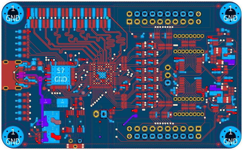
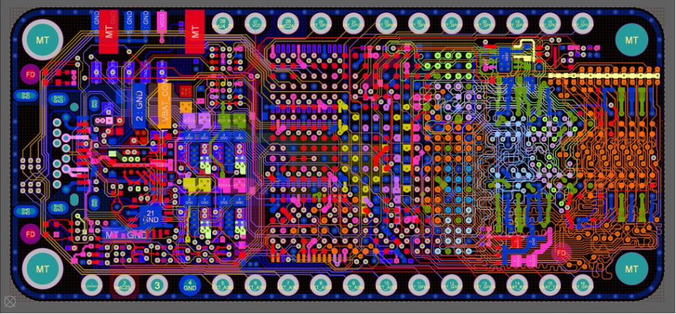
PCB Layout and Analysis:
KFTRONICS specializes in PCB Layout Design services for a wide range of complex boards, including multi-processor, MIL-STD-compliant, and highly dense small footprint PCBs. Our experienced team ensures world-class PCBA designs that are certifiable, high-performing, cost-effective, and thermally efficient.
With over 10 years of experience, KFTRONICS has been a trusted provider of custom PCB design and layout services to government, public, and private sectors in India. As a leading PCB design company in India, KFTRONICS specializes in high-speed digital and mixed-signal PCB layouts for various applications, such as consumer electronics, industrial, aerospace, and defense. Their services include custom PCB design and analysis for VME, VPX, cPCI, PCIe, XMC bus, and custom architectures.
PCB Layout and Design Service:
The PCB Design Workflow at KFTRONICS:
- Schematic Capture:
Schematic design is crucial for any project, as it forms the foundation for construction plans and electronic circuits. This guide delves into the essential principles and elements of schematic design, equipping you with the knowledge needed to navigate this pivotal stage. It translates initial concepts and requirements into a visual depiction, outlining the project's shape, purpose, and spatial connections. Essentially, it serves as a roadmap for the project's development.
- PCB LAYOUT:
A well-designed PCB layout is crucial for the success of any electronic device. It serves as a detailed map that directs the flow of electricity, influencing the functionality, performance, and reliability of the system. An efficient layout is essential for a seamless transition from design concept to a fully functional product.
Key benefits of an efficient PCB layout:
- Enhanced performance:
- Reduced electromagnetic interference (EMI):
- Improved thermal management:
- Simplified manufacturing:
- Increased reliability:
- Reduced size and weight:
Efficient layout techniques can result in smaller and lighter PCBs, making them ideal for space-constrained applications.
When designing a PCB, size is crucial as it impacts production costs. Larger sizes increase plate numbers, leading to higher impedance, longer printing lines, and maintenance costs. Conversely, overly small sizes reduce component spacing, affecting heat dissipation. Finding the right size balance is essential for optimal PCB design.
Heat dissipation affects product stability and lifespan. Close component proximity can cause integrity interference. Determining PCB size, placing components, and considering component types are crucial steps. Proper component allocation prevents interference and compatibility issues. A well-distributed layout enhances functionality, compatibility, and aesthetics. Balancing function and appearance in PCB layout contributes to successful PCBA design.
- DRC Checking:
Design Rule Check (DRC) is an automated process that ensures a PCB design adheres to specific constraints such as trace width, clearances, and hole sizes. DRC helps detect potential errors that may result in manufacturing defects and affect the reliability of the board.
PCB reverse engineering / PCB Cloning
Our Custom PCB Design services include PCB reverse engineering, re-engineering, and optimization of existing designs for cost and obsolescence management. Our experienced engineers help customers bring products to market faster with high performance and manufacturability. Our PCB Design Analysis Services cover Library management, PCB Layout and Analysis, Power Integrity, Signal Integrity, Structural Analysis, and Thermal Analysis
PCB reverse engineering involves extracting the design secrets of an existing printed circuit board. This process can be crucial for various purposes, including:
- Replicating existing designs: for repair or production.
- Analyzing competitor's products: to understand their functionality and gain technical insights.
- Creating modifications or improvements: to existing circuits.
RAPID PROTYPING:
At KFTRONICS, electronic circuits can be quickly prototyped on electronics prototyping boards before being printed on a manufacturing electronic circuit board (PCB). The purpose of these boards is to streamline the assembly process, allowing for easy component connections and circuit modifications.
Bringing your electronic circuit designs to life starts with a crucial step that is prototyping. Building a functional PCB prototype allows you to test functionality, identify design flaws, and refine your concept before committing to mass production.
Electronics Design Services:
Electronic products are essential in our daily lives, powering various technologies. Developing these products requires expertise in electrical, mechanical, and software engineering. Electronics design services help in designing, testing, and bringing electronic products to market efficiently. These services are provided by electronics design companies or ODMs to assist customers in creating innovative connected devices.
Our experienced team specializes in electronic design and manufacturing, with 90% having worked in leading industry enterprises. They have strong technical expertise in mobile phones, automotive electronics, and the Internet of Things. By analyzing industry data and market trends, we can guide technology and product development to meet customer needs effectively.
KFTRONICS has over 10 years of experience in high-end consumer electronics, financial POS, three-proof equipment, automotive electronics, and other industries. Specializing in ARM architecture, we lead the industry in image processing, low power consumption, system optimization, intelligent voice acquisition systems, and audio processing.
Electronic design services involve a series of stages essential for transitioning from concept to final production. This process includes designing, innovating, creating, and manufacturing electronic products, known as electronic design development. Electronic design companies usually follow these key steps in the electronics design services manufacturing and assembly process:
Requirements Analysis:
Electronic design services encompass the crucial stages of transitioning from concept to final production. This process involves designing, innovating, creating, and manufacturing electronic products, collectively known as electronic design development.
Concept Development:
Electronic design companies typically follow these key steps in the electronics design services manufacturing and assembly process: Conceptualization, Design, Prototyping, Testing, and Production.
System Architecture Design:
This phase focuses on the system architecture, encompassing both hardware and software components. Key activities include:
- Creating circuit diagrams
- Defining APIs/interfaces between subsystems
- Designing firmware architecture
- Modeling mechanical structure
Budget Estimation:
This stage involves calculating the expenses and budget for the production and manufacturing process. Early budget estimation is crucial to ensure that the product can be designed and produced within the budget constraints while remaining profitable. Budget estimation plays a key role in electronic product design.
With our multilevel supply chain management, we can efficiently source electronic components globally at competitive prices. Our services are cost-effective and accessible.
Hardware & Software Design:
In this phase, the system architecture blocks are detailed. Hardware design includes PCB layout, part selection, and simulation. Software design involves coding modules, unit testing, and integration testing. We can deliver a rapid prototype Proof of Concept (POC) within two to three weeks.
Validation and Verification:
Electronic design validation and verification ensure that the electronic system or device meets specified requirements and functions correctly. Prototypes undergo thorough testing to verify compliance and identify defects. Tests such as HALT, EMI/EMC, and environmental tests validate robustness. Validation ensures that the final product meets customer demands and includes field testing, system testing, reliability and performance testing, and regulatory compliance.
Electronics Manufacturing:
This phase is crucial in electronic design services as it involves transitioning the product to production. This includes selecting component suppliers, assembly partners, and collaborating closely to scale up manufacturing.
Certification and Documentation:
Certification is essential for electronic products sold globally. Products must comply with safety and emissions regulations such as UL, CE, and FCC. Certification processes run concurrently throughout the design phase.
Production Sustenance:
After the launch, the provider offers support for failure analysis, upgrades, optimizations, and other necessary services throughout the production lifecycle. This encompasses the entire electronic design and manufacturing process.
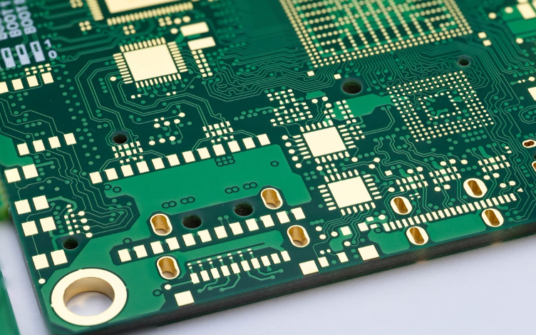
PCB fabrication
KFTRONICS partners with multiple vendors to provide efficient PCB fabrication services. We carefully select vendors based on factors such as PCB finish (HAL, ENIG, IMMERSION GOLD), gold and copper thickness, production volume, quality expectations, trace thickness, hole sizes, and quality control measures. Effective quality control in PCB manufacturing leads to improved reliability, cost savings, and reduced defects. Manufacturers should prioritize quality control to ensure the final product meets quality standards and performs reliably in the field.
We specialized in following PCB Fabrication services
· Rigid PCB – 0.5 – 2.4mm Thickness
· Rigid PCB HAL finish
· ENIG finish/ immersion gold
· 1 Layer- 16 Layer
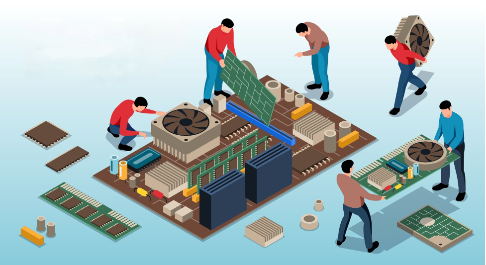
PCB Assembly
As one of the best PCB manufacturers in India, our goal is to provide our customers with the best quality products and services at the most competitive pricing, and to become a reliable long-term partner of our customers in PCB manufacture and assembly.
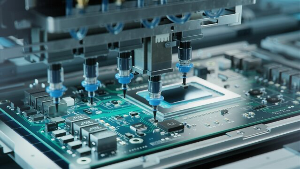
Since its establishment in 2015 as a printed circuit board manufacturer, KFTRONICS Technology has focused on high-quality, low to medium-volume PCB fabrication, PCB Assembly and electronics manufacturing.
Our products and services include Multi layers printed circuit boards, through-hole assembly, SMT Assembly including BGA assembly, components sourcing, and turnkey box build and electronic product development.
At KFTRONICS, “Total Customer Satisfaction” is our goal, and it is the core of our operation as a PCB manufacturer. Procurement, sales, engineering, manufacturing, inventory, and quality have the same common goal of ensuring directly or indirectly “Total Customer Satisfaction”. We aim to become one of our customers' most trustworthy printed circuit board manufacturers.
Our core competitiveness is high-quality products and fully-flexible & fast response. Therefore, our engineering and procurement team fully cooperate to give customers the best support and quote the best price; our production and quality team regard the quality of product as the most critical indicator; our customer service team and the entire company regard flexible meeting the diverse needs of customers and quick response as our Habit.
PCB Assembly
- SMT Assembly
- Through Hole PCB assembly
- Prototype PCB Assembly
- Custom PCB Assembly
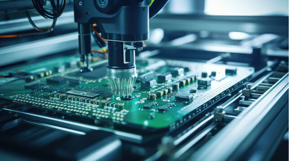
SMT Assembly
Do you know exactly about SMT assembly? Why not learn more about SMT assembly by taking a glimpse at this article?
SMT is shorthand for Surface Mount Technology. It is about the process of assembling the components on the surface of the printed circuit board directly. It is different from PTH Assembly. PTH assembly is plated through hole assembly, which means we plug the component pins in the PCB hole first and then solder the pins in the holes.
Because today the electronic industry develops so fast, electronic products become smaller and more complex. To adapt to such a trend, engineers adopt the method of SMT assembly/SMT manufacturing. When some people take a look at the printed circuit boards with components of electronic products (smart phones, computers, medical electronics, telecommunication electronics or car electric parts, etc.), they may wonder how these components are mounted on the boards. Let’s reveal the answer they are mounted by the SMT assembly.
When you search pictures of SMT assembly factories, you can find out the prevailing presence of advanced automatic pick & place machines.
- The products need to be designed as small as possible
Because a lot of products on the market demand become smaller and smaller now, such as smart phones, cameras, wearable electronics, GPS trackers, blue tooth earphones, etc. That’s the reason why the electronic components used to make those products also become smaller and smaller.
- The efficiency of SMT assembly is much higher
As we all know, the automatic pick and place machine can run very fast, print solder on the PCB, run through the reflow oven, then the SMD components soldering is done! It is so easy and quick.
But for PTH assembly, PTH components need to be plugged into the PCBs holes one by one first, and the lead legs also need to be cut after PTH assembly.
This is very time-consuming. So the production lead time is quite long for large production if PTH assembly is used.
- SMT assembly is more cost effective
Since the SMT assembly has high efficiency, it is more cost-effective. As for PCB Bare Board, the PCB cost would be also a little cheaper since there are fewer drills. And the lead time is also better.
- Easier to get a high yield with good quality
In SMT assembly, all the processes are done by equipment. So there is less chance of making mistakes. In addition, for seeking high-quality products, inspections are required. AOI inspection is one of the most commonly used inspections.
Through Hole PCB assembly
Through-hole PCB assembly is a method of assembling electronic components onto a PCB. Through-hole components are those that use metal leads or pins that are inserted into holes drilled into the board. Through-hole assembly utilizes manual labor and is typically used to assemble more significant, heavier components with higher pin counts.
In addition, it allows for more reliable connections on the board, as it requires components to be soldered or crimped into place. Through-hole PCB assembly is also more tolerant of physical stress and vibration than other assemblies. By the way, KFTRONICS provides high-quality through-hole PCB assembly, which is often used in industrial and commercial applications where reliability and durability are paramount.
Features of Through Hole PCB Assembly
- Through-hole PCB assembly allows components to be directly connected through drilled holes and soldered on both sides of the circuit board.
- Through-hole technology is suitable for producing complex, large-scale circuits in high-frequency applications.
- Through-hole components can handle heavy current loads due to their larger size and more reliable connection points than surface mount boards (SMT).
- Through-hole PCBs are able to support heavier components such as connectors, potentiometers, and switches etc., which are typically not compatible with SMT assemblies.
- Through-hole boards have more excellent heat dissipation capabilities compared to SMT's as they allow a greater area of contact between the component and circuit board via metal plating or soldering techniques.
- Through-hole technology offers better electrical performance in terms of signal integrity, EMI shielding & ground plane designs when compared with other technologies like SMD/SMT.
- Through-hole boards offer easier reparability than surface mount technology because they give both sides easy access for rework and repairs.
- Through-hole technology offers more excellent reliability than surface mount technology due to its robust mechanical connections. Therefore, it is ideal for applications where maintaining a secure connection is paramount.
- Through-hole boards have greater tolerance of temperature, shock and vibration than SMT due to their larger size and strength of electrical connections, making them ideal for applications where these parameters are essential.
Advantages of Through Hole PCB Assembly
Humans use electronic devices for their own sake, and our interactions with them are often not gentle. We tend to drop them, turn them on and off frequently, and treat them roughly, which easily damages them. Through hole can solve this problem.
So we need to find a type of PCB which can withstand this rough usage. And we find out the best way to make durable PCB boards is through hole technology assembly. Through-hole components with a long lead then use them to assemble the PCB board. We need to insert their lead into the PCB hole.
Using through-hole components, we can make out stronger bond PCB board than standard metal-based components because through-hole components are all with lead, which can be run through the hole of the PCB board, and then solder together. This structure makes the board and component joint more firm. It makes the PCB board work better under environmental stress. Some large, high-power and heavy components must be mounted on the PCB board with through-hole technology such as a transformer.
Through-hole components are commonly used in various industries, such as aerospace, automotive, and military. They are ideal for rugged, durable components to work in harsh environmental conditions, such as collisions or extreme accelerations. Through-hole components can also be used for prototyping and testing.
Prototype PCB Assembly
When a PCB is designed by an engineer, no one can assure it will be functionally well 100%. So a few prototypes are always needed to avoid big losses in mass production if there are any design errors. The quantity is around 1 to 100 pcs normally. We call this prototype PCB assembly.
Besides, Prototype PCB assembly may also be needed to evaluate a new supplier, even if is it a mature product. Since there is a potential risk if moving an existing product to a new supply.
Prototype PCB Assembly Process Steps
The application of solder paste
First, the solder paste (a small particle of solder paste mixed with flux) is applied to the circuit board. For this application, most PCBA manufacturers use stencils (They are available in several sizes. Shapes and specifications are in line with the specifications), which can only apply the correct amount of solder paste to certain parts of the circuit board correctly.
Component placement
Unlike in the past, this stage of the PCB assembly process is now fully automated. The picking and placing of components (such as surface-mounted assemblies), once done manually, is now performed by robotic pick-and-place machines. These machines place components accurately into pre-planned areas of the circuit board.
Reflow soldering
Now the solder paste and all surface mount assemblies are in place. What's your next step? Curing the solder paste to the correct specifications is critical to properly adhering the PCB components to it. This is the relevant part of the PCB assembly process - reflow soldering. To do this, the assembly with the solder paste and the components on it is passed through a conveyor belt, which passes through an industrial-grade reflow oven. Heaters in the oven melt the solder in the solder paste. Once the melting is complete, the assembly will again move through the conveyor and be exposed to a series of cooler heaters. The purpose of these coolers is to cool the melted solder and allow it to cure.
Inspection
After the reflow soldering process, the PCB should be inspected to check its functionality. This stage helps identify poor-quality connections, misplaced components, and shorts due to the continuous movement of the board during the reflow soldering process. PCBA manufacturers use multiple inspection steps such as manual inspection, automated optical inspection, and X-ray inspection to check the functionality of the circuit board, identify lower-quality solder and identify any potential pitfalls. Once the inspection is complete, the assembly team will make the critical decision. Circuit boards with several functional errors are usually scrapped. On the other hand, if there are smaller errors, the circuit board is resent for rework.
Insertion of through-hole components
Certain types of PCBs require the insertion of through-hole components along with conventional SMD components. This stage is dedicated to the insertion of such components. For this purpose, the signal is passed from one side of the circuit board to the other with the help of those PCB components to create plated through-hole. Through-hole insertion of PCB is usually done by manual soldering or wave soldering.
Final inspection
Now it is time for the second level of inspection. Here, the PCB assembly is tested for functionality, or the PCB assembly is thoroughly inspected to monitor its electrical characteristics, including voltage, current or signal output. Today's manufacturers utilize a variety of advanced test equipment to help determine the success or failure of the finished PCB assembly.
Cleaning
Because there is a lot of flux left on the PCB during the soldering process, it is critical to thoroughly clean the PCB assembly before delivering products to the customer. For this purpose, PCB assemblies are cleaned in deionized water. After the cleaning process, PCB assemblies are thoroughly dried with compressed air. The PCB assembly can now be prepared for customer inspection.
Why Choose KFTRONICS for Your Custom PCB Assembly Requirements?
KFTRONICS fully implements a strict enterprise management system, from production and sales to after-sales service in all aspects of institutionalized, process-oriented, standardized and systematic operation, and strictly implements the international quality system standards to ensure the rigorous process of the enterprise.
Over the past 10 years, with high-quality custom PCB assembly, a good reputation and excellent service, we have won unanimous praise from our customers. We will try our best to meet the various requirements of customers with high-quality products, reasonable prices, high speed and efficiency. We always adhere to the user first, serve our customers with heart and soul, and insist on impressing our customers with our service.
We are confident that our commitment to quality service and unsurpassed customer support make us the ideal choice for your PCB Assembly needs. With our advanced machines, skilled professionals, and years of experience in the industry, we can guarantee that we will handle your project with precision and accuracy.
Rigid PCBs can be divided into the following three categories.
- Single-sided PCBs
- Double-sided PCBs
- Multi-layer PCBs
Single-sided PCBs
Is the Single Sided PCB’s the simplest type of PCB in the PCB industry? Of course. The copper traces only exist on one side, and there are no plated-through holes. It is used in very simple electronic products normally, such as power PCB, led PCB, and PCBs for household appliances. Some people may ask: “Is the metal core PCB also usually single-sided PCB?” The answer is obviously “Yes”. For example, aluminum PCBs which are widely used in the LED industry are also usually single-sided.
Double-sided PCBs
For Double Sided PCB’s, the circuits are placed on both sides and the dielectric is in the middle of the board. Both top and bottom layers can be connected by the plated through holes. Most of the double-sided circuit boards are simple, but some 2-layer PCBs are very complicated, with less than 4mil copper traces and 8mil drill sizes.
So more functions can be realized in double-layer PCB. Someone may ask, “Can the power supply PCB, inverter PCB, amplifier PCB, energy meter PCB, and control PCB be double-sided PCB?” The answer is obviously “Yes!” Some may not believe that more than 50% of rigid PCBs are double-sided PCBs. But that is the case.
Multi-layer PCBs
Regarding the definition of multi-layer PCB, many people will grab the answer, “Multilayer PCB is a circuit board with more than two conductive layers, right?” Yes, they are right!
Most multilayer printed circuit boards are even number layers; the symmetry helps to keep the PCBs flat, to reduce the change of bow ad twist after production. We add one or more power plane layers or signal layers in the middle, to achieve more integrated functions in one printed circuit board, and also possible to produce copper trace width and space, drill size, etc.
Multilayer circuit boards are mainly used in electronic devices with complex functions and also need to be small in size, such as industrial control, telecommunications, medical, 5G base stations, computer peripherals, IT servers, automotive electronics, desktop computers, etc. Multilayer circuit boards generally range from 4 to 16 layers, and very complex ones may exceed 100 layers at most.
Flexible PCB
A flexible printed circuit board also called a soft board or a flex PCB, is made of a flexible insulating material circuit board. Its biggest feature is flexibility, able to bend and rotate freely.
Flexible printed circuit board selection of insulation substrate commonly used there are two: polyimide (PI) or polyester (PET) film.
- Polyimide is an organic polymer material with excellent comprehensive performance, with high-temperature resistance up to 400°C and high thermal stability and flexibility. Polyimide flex PCB material is the most widely used flex PCB material, such as Smartphone, wearable devices, automotive electronics, cameras, automation, robotics, medical, aerospace, military electronics etc. Besides, because of it higher temperature resistance, PI flex PCB material can be used in the dielectric substrate of solar cells and LED lamps and lanterns. The lamps and lanterns will generate a lot of heat under long-term high-temperature conditions, and only the flex circuit can work normally for a long time.
- Polyester film is also a kind of high polymer material, with good mechanical and thermal stability, but cheaper cost than polyimide (PI) material. It is widely used in consumer electronics and automotive industry.
Rigid Flex PCB
The Rigid-flex printed circuit board refers to the rigid printed circuit board and flexible printed circuit board combined after pressing and other specific processes. At the same time, it has two characteristics: rigidness and flexibility. We can assemble many electronic components on the rigid part and bend the flex part to achieve the usage purpose after the final assembly at the same time.
Rigid flexible PCBs are widely used in high technology electronic products, such as industry, automation, medical, telecommunication, wearable electronics, automotive, IoT, robotics, military, aerospace. Kftronics is one trustworthy rigid-flex PCB manufacturer with 16+ years of experience, so you can rely on us to produce your rigid-flex PCBs in highest industry standards and competitive pricing. Please contact us our sales team freely to get a cost of rigid flex PCB immediately.
HDI PCB
HDI PCB stands for High-Density Interconnect PCB. If someone knows that HDI PCB is a circuit board designed to have high-density connections and components while minimizing board size, then we can tell he knows a lot about the PCB industry.
When referring to traditional PCBs, one would think that it would be impossible to use advanced manufacturing techniques and materials to achieve higher levels of complexity and functionality. However, high density PCBs can do this. This is accomplished by incorporating multiple layers of conductive traces and vies in a much smaller space, allowing for more components and circuitry to be integrated into a single board.
There is no reason why advanced electronic devices such as smart phones, tablets, medical devices and high-end computing devices should not use HDI PCB manufacturing. These devices require a high level of functionality, miniaturization, and performance in a small form factor, making high density PCBs an essential component in their HDI PCB design.
HDI PCB board representative is one of the quick development technologies in PCB and PCBA process. If you know, it is a relatively high-density line distribution circuit board using micro-blind and buried-hole technology, and then it means you are very concerned about the development of PCB industry technology.
Aluminum PCBs
If someone knows that aluminum PCBs are a particular type of PCB that uses aluminum as a substrate, then we can tell that person knows a lot about the PCB industry. For example, some familiar with the PCB industry may say, “These PCBs are commonly used in applications that require high thermal conductivity, heat resistance, and durability, right?” Yes, you got the point.
If someone says that, like fiberglass or plastic substrates, Aluminums PCBs are susceptible to scratches, cracks, and other physical damage, that statement is false and very different from the truth. They are used in various products, from LED lights and power supplies to automotive signaling and lighting, smart home applications, aerospace, and medical devices. They are becoming increasingly popular due to their excellent thermal conductivity and consequent ability to dissipate a high heat level, improving product lifespan and reliability.
In short, if Aluminum printed circuit boards do not provide higher performance and more excellent durability, then projects for these electronic applications will have difficulty succeeding.
Multilayer PCB
As the name of multilayer PCB, the difference between multilayer PCB and single and double side PCB in essence, is that their number of layers is not the same. But, of course, multilayer PCB has more layers, and the number of layers of multilayer printed circuit board is in three or more layers.
KFTRONICS has rich experience in production and cooperation, both single panel and dual panel, including multilayer PCB board. They are the same when it comes to connecting circuits.
According to our production experience, most are connected by the through hole on the board unless there are special requirements and circumstances. This is because the production principle of multilayer PCB manufacturing is very different from the traditional production method.
The multi-layer PCB is drilled and electroplated before rolling synthesis. Based on our experience, the inner part is usually assembled from traditional double-sided PCBS. The outer layer is different from the inner layer, which comprises individual single panels. Before being pressed together, the inner double-layer PCB has undergone the usual production steps, such as drilling, plating, etching, etc.
Usually, based on the production experience of our, the outer layer is drilled with a signal layer. Then the several layers are pressed together to achieve a multi-layer PCB. KFTRONICS has many options for pressing multilayer printed circuit boards, such as hydraulic presses or pressure pods.
If Our presses multilayer PCBs with a hydraulic press, preheat first and then place the multi-layer PCB material to be pressed into the preheated pressure. Eventually, it changes the material from a rigid state to a sticky form.
PCB Prototype
PCB Prototype is a circuit board that has been designed and manufactured to test the functionality of a design before it goes into mass production. PCB Prototypes are typically used in product development, where engineers can quickly and easily make changes to their designs based on initial testing results.
Metal Core PCB
A metal core PCB is a pcb with a metal substrate to be a substitute of FR4 which is the most commonly used PCB laminate. MCPCB always contains three layers: base metal substrate such as aluminum, copper etc., then a dielectric and a copper layer to etch traces. This metal substrate is always used to dissipate heat from electronic components. The most commonly used substrate is Aluminum, but there are also Copper, Iron and other alloys.
Custom PCB
Custom PCBs are specifically designed and tailored to meet the specific requirements of electronic devices. They are created through PCB prototyping, which involves developing a layout for the PCB and manufacturing it using specialized equipment. Custom PCB boards can be designed in any shape or size and can incorporate a wide range of components, including resistors, capacitors, and integrated circuits.
Custom printed circuit boards are often used in applications where standard PCBs cannot meet the specific requirements of the electronic device. For example, custom PCBs may be used in medical devices, aerospace applications, or military equipment, where the reliability and performance of the electronic device are critical.
Gold Finger PCB
Gold Finger PCBs are specialized printed circuit boards characterizing gold-plated fingers, or contacts, along one edge of the board. They are often used in high-end electronics due to their superior electrical conductivity and reliable signal integrity.
Gold finger PCBs are also highly resistant to corrosion and oxidation, which makes them ideal for long-term use in harsh environments. Furthermore, gold fingers provide a low contact resistance when connecting with other components on the board or external cables.
Since edge connector PCBs offer many advantages over traditional circuit boards, they play a crucial role in various applications such as consumer devices and aerospace technologies.
Impedance Control PCB
The conductors in the circuit board will have various signal transmissions. To improve its transmission rate and increase the frequency, the line itself, due to etching, lamination thickness, wire width and other factors, will cause changes in impedance value, causing signal distortion. Therefore, the conductor on the high-speed circuit board’s impedance value should be controlled within a specific range, called “impedance control”.
As the name implies, an controlled impedance PCB is a printed circuit board designed to control electrical impedance. Accurate transmission of signals between components can be well achieved in the impedance control PCB. They also reduce power consumption by preventing signal loss due to reflections or interference while providing a cost-effective solution for many applications. Impedance-controlled printed circuit boards ensure efficient data transmission in complex electronic systems.
Why Choose Us:
- Competitive Pricing
- Great Customer Service
- On-time Delivery
- No MOQ & Quick Turn Production
- One-Stop Turnkey EMS Service
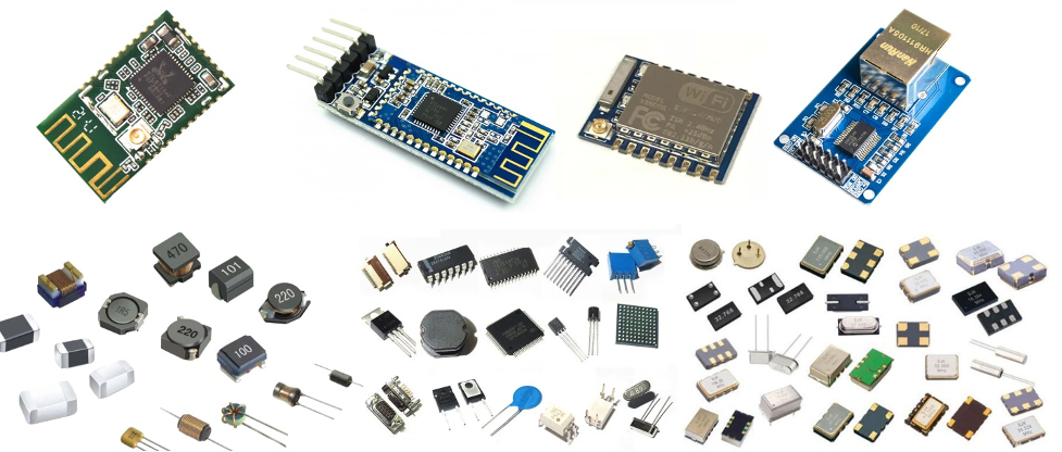
Component sourcing:
Unless an OEM is one of the few that is vertically integrated with manufacturing, the general considerations for PCB and PCA sourcing decisions and the criteria that should be used to evaluate and select suppliers are left to the purchasing department.
Needs assessment
- Engineers start by assessing the requirements of the project based on the specifications. They determine the type and quantity of components required for new product development.
- Valuable information is provided by preliminary engineering drawings and product designs.
- Working with the finance and business development teams helps to establish a budget and a detailed bill of materials (BOM).
Strategy development
- Several critical tasks are involved in this phase:
- Primary and secondary supplier selection.
- Collection of data on part numbers, descriptions and pricing.
- Review bill of materials for consistency and accuracy.
Developing and contracting supplier relationships
- Vendors are approached for business once the documentation is complete.
- Negotiating and signing service level agreements (SLAs) are part of building strong relationships with vendors.
- Companies may work with multiple vendors at the same time.
Sourcing Channels
When it comes to procuring electronic components, you have several options:
Buy direct from manufacturers
Manufacturers produce and stock components in large quantities.
Advantages
- Short supply chain: Orders are fulfilled more quickly.
- Technical support and customer service.
- Access to authorized distributors.
As a specialist in the procurement of electronic components, your role is crucial in ensuring a seamless flow of components from production to use. By understanding the dynamics of the supply chain and implementing cost-effective strategies, you can make a significant contribution to successful product development.
Remember, every resistor, capacitor and microcontroller plays a vital role in powering the devices we rely on every day.
Electronics testing Services
Organizations are demanding quality at speed and scale as they look to software as a source of competitive advantage. They need to rethink how they build and test applications, moving from testing as a standalone function at the end of the development cycle to embedding quality throughout. With an intelligence- and insight-driven approach, our Quality Engineering services are designed to drive speed, quality and productivity. We have the skills and capabilities to help you succeed, whether you want to bring new software to market faster or transform your test function and workforce. Our goal to ensure that applications don't just 'work’, but deliver a differentiated user experience.
Unit Testing:
Purpose: Unit testing is used to verify the correctness of individual modules or components within your software application. Each unit (such as a method or function) is tested in isolation to ensure that it performs specific tasks as expected.
Benefits:
- Early detection of bugs or issues in the code.
- Developers gain a basic understanding of each unit, enabling faster modifications.
Cost and Maintenance: The cost and maintenance of unit testing are relatively low.
Number of Test Cases: Unit testing involves a higher number of test cases compared to functional testing
Functional Testing:
Purpose: Functional testing is the validation that the software system will function efficiently in accordance with the functional requirements. It ensures that each function works correctly based on the specified requirements and specifications.
Benefits:
- Identifies defects in the system that may have been missed during application development.
- Provides insights into the quality of the output data.
Cost and Maintenance: The cost and maintenance of functional testing are relatively high.
Number of Test Cases: Functional testing involves fewer test cases compared to unit testing
In summary, both unit tests and functional tests play crucial roles in identifying defects, preventing issues, and ensuring the delivery of a quality product. While unit tests focus on individual components, functional tests validate the overall system behavior from the user’s perspective.
Enclosure Services and Automation Solutions
Precision, safety and reliability are paramount in the dynamic landscape of industrial automation. Kftronics, India's leading manufacturer of stainless steel enclosures. Kftronics has a rich heritage in providing high quality enclosures. They combine functionality, durability and regulatory compliance to protect your valuable equipment.
Customized enclosures
To meet your needs, Kftronics designs enclosures. Whether it's a control panel, distribution box or meter box, their experts will create solutions that fit seamlessly into your workflow. Choose from optional welded or bolted structures with removable sides for easy access.
Robust construction
- Wall mounted enclosures: These enclosures optimize space utilization and are available up to 1500mm high.
- Outdoor Canopies: For protection from the elements, Kftronics offers canopies for outdoor applications.
- Concealed hinges: For hassle-free maintenance, the wide 120-degree opening allows for easy removal.
- Sturdy mounting brackets: Direct wall mounting made safe and easy.
- IP-65 rated ingress protection: Designed for increased durability to protect critical equipment.
Top applications
Kftronics enclosures are used in a variety of applications:
- Starter boxes: Efficiently house motor starters and control circuits.
- Distribution boxes: Organize electrical components for seamless power distribution.
- Terminal boxes: Secure connections and facilitate maintenance.
- Remote control and monitoring boxes: Allow remote monitoring and control.
- Meter boxes: Securely house energy meters and monitoring equipment.